Un-killable microSD Card
In a previous post, I was talking about getting FatFs1 up and running on a custom board. However, I was having issues related to the power supply. My first hint was investigating if there were power fluctuations and if the SD was being provided the proper amount of power through the switch. This was my initial thought because the first block read would work while following reads and writes wouldn't.
Hardware: High Side Switch
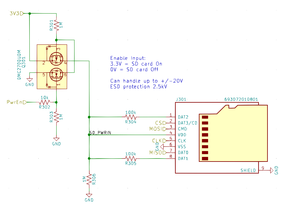
In my boards, I have always liked to engineer in high side power switches. What this usually translates to, is a main high-side P-FET acting as the power switch, which is controlled by a low-side N-FET. High side switches are particularly useful in the fact that no current flows after the switch unless it is on. So, in the case of an exposed connector this is ideal. No live voltage is exposed until the switch is activated.
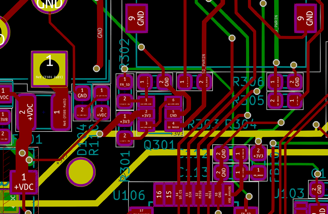
Fet Board Layout
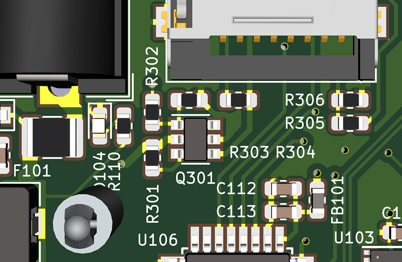
Fet 3D Rendered Layout
As seen above, I use a handy complementary pair mosfet, which integrates a P-MOS and N-MOS in a single package, pull up/down resistors for the gates, and a series current limiting resistor for the N-MOS gate to implement the high side switch.
I have chosen this configuration for several designs because it operates as an active-high switch. Meaning the default state of the switch is off, unlike a mere P-FET. Also, the DMC2700UDM used here is mere $0.35 in single quantities and $0.12 at quantities above 100.
Doing the math out for giggles, R302 and R303 form a resistor divider with the gate of the N-CHANNEL — Q1. According to the datasheet, the first load line is for 3.3V Vds is Id=200mA at Vgs=1.2V. For guaranteed operation, the output of the divider at the gate must be greater than this voltage. The standard formula for a resistor divider is as follows:
1Vgs = (Vin * R2 / R1 + R2 ) = (PwrEn * R303) / (R302 + R303) = (3.3 * 1000) / ( 10 + 1000) = 3.267 V
As expected with a 1/100 divider ratio, the gate sees 99% of the PwrEn GPIO voltage. With this, there is absolutely no chance for resistor or part tolerance to effect the turn on of the P-FET with a GPIO voltage > 1.21 V.
After probing the output of high side switch at SD_PWRIN with my oscilloscope, I realized there was no power rail drooping and the rail was accurately holding at 3.28V, well within spec of the SD card. From this, I was able to eliminate the switch and my switching buck regulator. I had to dive in deeper...
Power Up Sequence Debugging
When I continued to probe the SD card through operation, I realized that the rail never went below ~2.7V. This immediately caught my attention. Intuitively, I knew there was nowhere near enough capacitance on the rail to hold it. Something else had to be supplying current to it. From the section above, I was confident in the switches doing their job. The high side switch was not supplying the power.
I needed to better understand this, so I created a small program to simply run through the following procedures with 1s delays between:
- Initialize the microcontroller and HAL libraries
- Clocks
- SPI
- Peripherals
- Turn on the SD card switch, PwrEn = high
- Turn off the SD card switch, PwrEn = low
- Deinitialize the microcontroller and HAL libraries
- Disable SPI controller
- Configure all GPIO as High-Z inputs
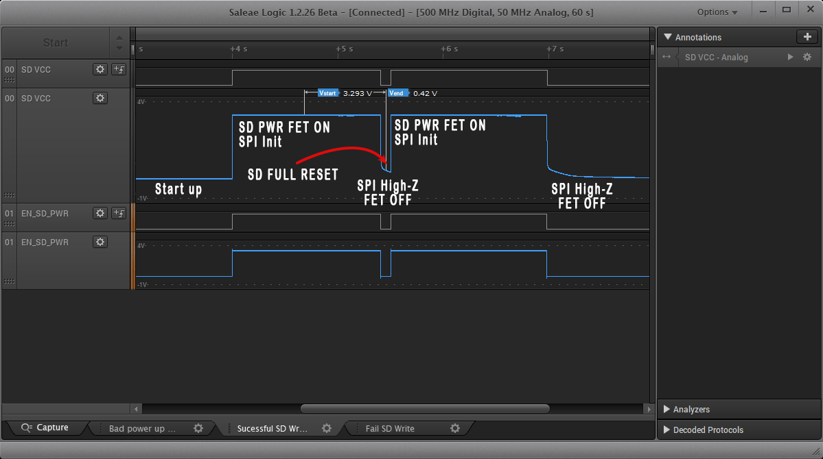
After attaching my logic analyzer, I could more easily navigate the mixed signal issue. I was presented with the following waveform:
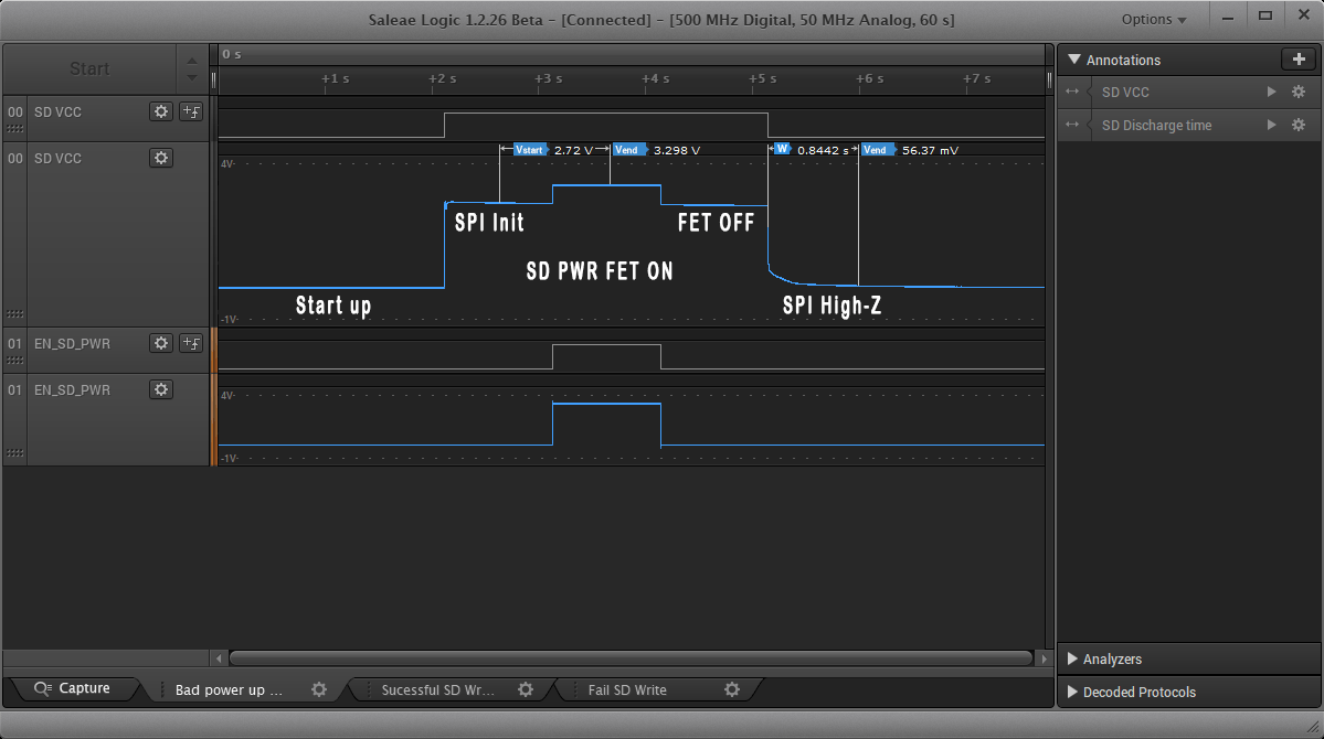
Instantly one can see that whenever the SPI peripheral is configured, the SD_PWRIN/SD_VCC rail never drops below 2.7V. Once I saw this I immediately knew my mistake.
Hint: 3.3 – 2.7 = 0.6 V. Likewise a standard silicon diode has a forward voltage drop of 0.6-0.7V
CMOS Protection
I have seen the "equivalent electrical circuits" of GPIO's in datasheets in the past and neglected that, creating this issue. Why would an SD card be any different? They are not. CMOS devices add clamping diodes at all inputs going to VCC and to VSS in order to protect the inputs from over-votlage and ESD. Digi-Key has a great article here demonstrating some techniques.
Digging around, I was able to find a datasheet for an SanDisk SD card, directly inside one can see the CMOS clamping diode going to VDD.
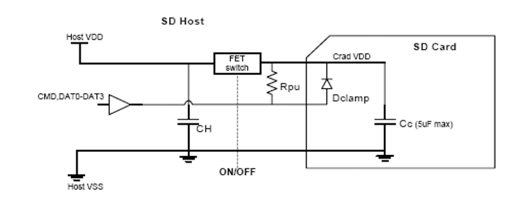
Note: Because there are clamping diodes on the CMD, CLK, and DAT0-3 pins, it is crucial to ensure that CLK, CMD, and DAT0-3 are at zero (0) volts during the delay and before the FET switch is turned on. If any I/O pin, (CMD, CLK, or DAT0-3) goes above zero volts during the delay and before power reaches the card VDD pin, it will forward bias the clamping diodes and can cause the card to go into an unknown state. It is the host's responsibility to make sure power gets to VDD before CMD, CLK, or DAT0-3 go above zero volts.
— SanDisk OEM Product Manual Document No. 80-36-03335
Hmm that sounds familiar. So really what was happening here was that through initialization, the microcontroller was activating the SPI data-lines which, in their idle state, were directly being shorted to the SD card's VDD through a clamping diode, Dclamp.
Through that process, one diode drop is applied and the SD card is still able to power on through these clamping diodes. Explaining the 2.7V VDD measured earlier. This works for a while, however, once a block read is issued the GPIO pins are not able to source the required current (on the order of 100mA) and the card browns out.
Additionally, this ghost powering through the GPIO prevents the card from being power cycled by the FET alone. The GPIOs need to be high impedance AND the power needs to be removed. Once this feature was added, the FatFs library yields the following correct waveform:
As with most problems, the solution can often be found in simply reading through the documentation and methodically debugging. I am very glad I went through this process of debugging this SD card as I am sure to never make the mistake of ghost powering devices again. Other communication schemes are susceptible to this as well, I2C is high on idle as well as standard Serial. These all have the potential to source current back into low current devices and power them.
Additionally, I must note that FatFs did have comments in the
power_on()andpower_off()driver functions suggesting the above functionality be implemented. This post describes an issue I personally created for myself by not reading the SD card datasheet and not fully implementing the SD card driver.
-
FatFs C library, http://elm-chan.org/fsw/ff/00index_e.html ↩︎