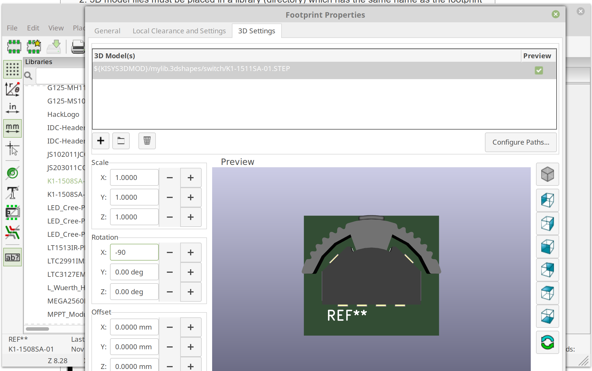
The K1-1508SA-01 is a multi-directional switch perfect for adding cheap navigation functionality to designs. I was unable to find any 3D models or detailed footprints, so I created my own.
As usual, it all starts with the datasheet...
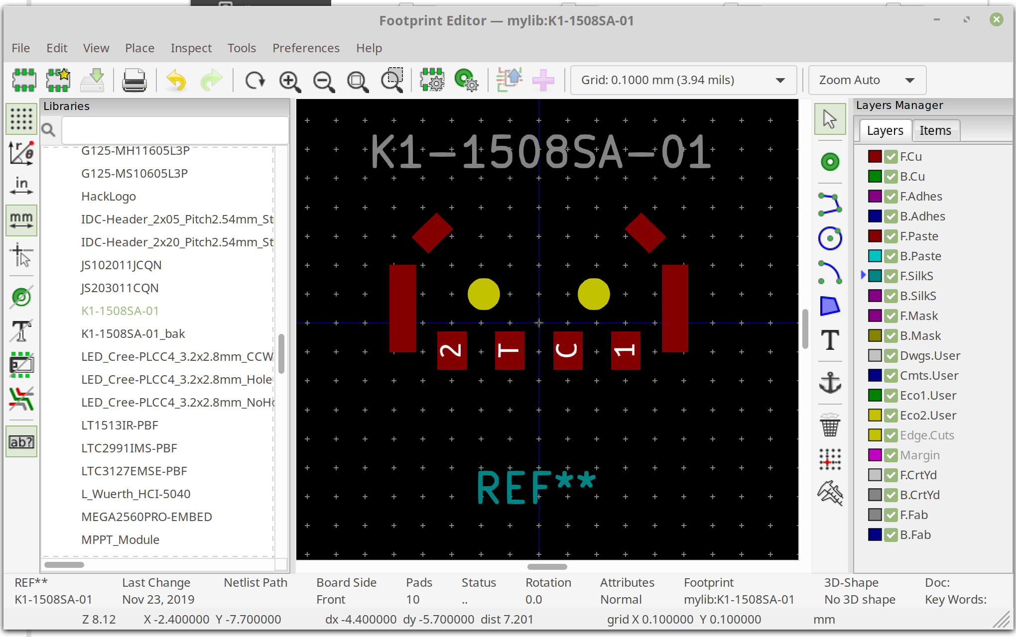
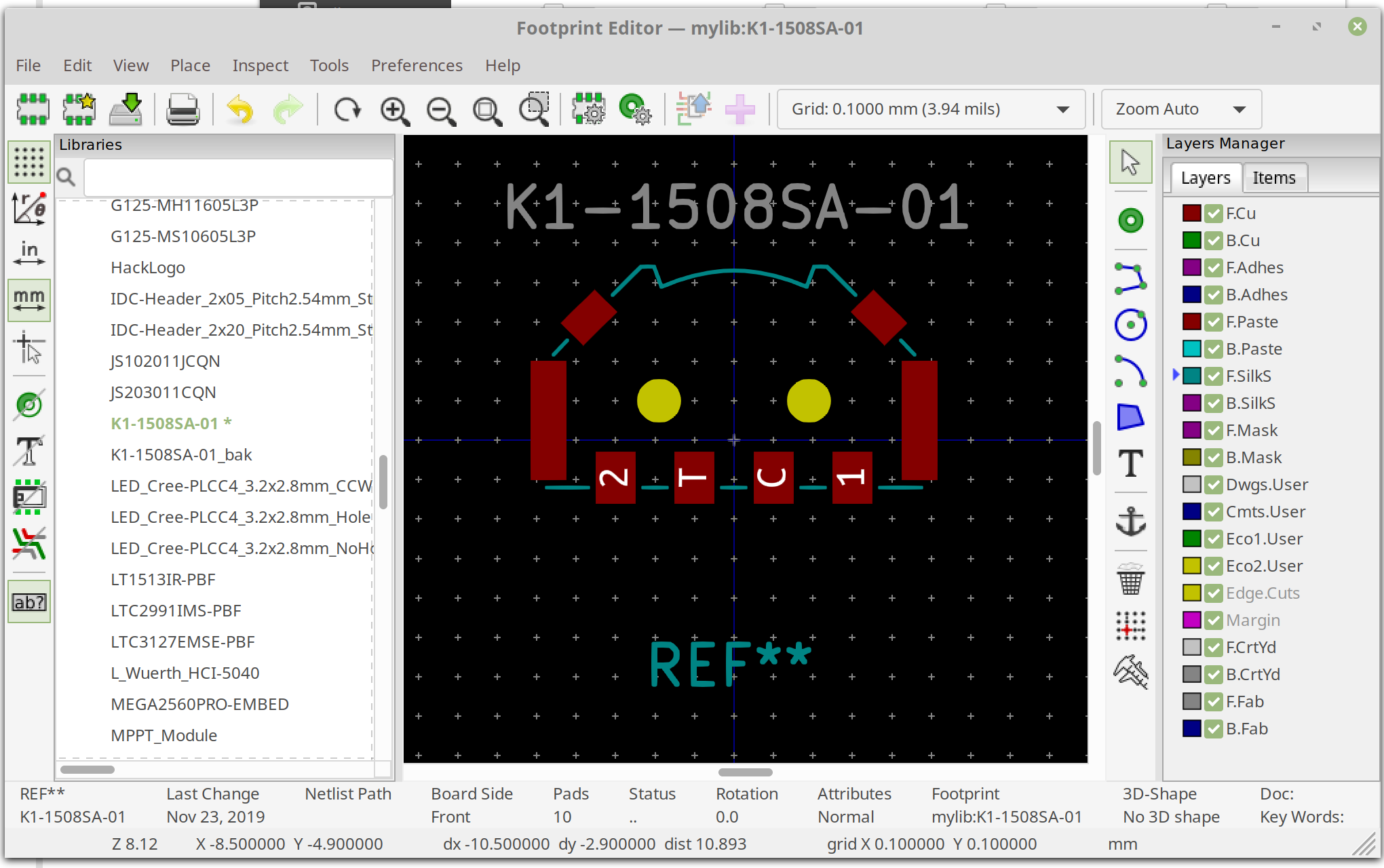
From here, I created the PCB land pattern in KiCad as described above.
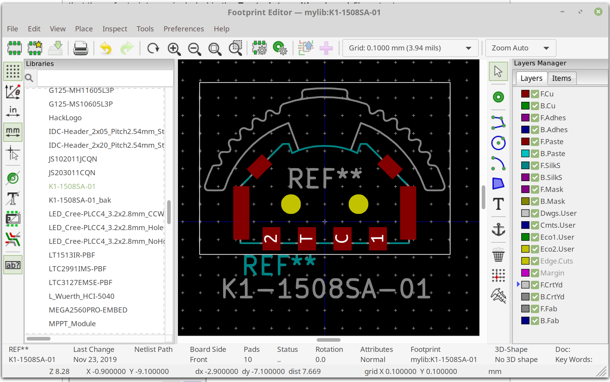
At this point, I normally would add in the silkscreen alignment and fabrication layers. However, upon closer inspection it can be seen that aspects of the both the mechanical and electrical design were left out in the datasheet. This, combined with the fact that I plan to design an enclosure around this device means that it would be best to go straight into the SolidWorks CAD design stage. More detail to come soon.
Example: Where is pin 3?
The pins are labeled 2, T, C, and 1. From that (along with one's engineering hat) one can deduce that C is for Common while T is potentially for Tap.
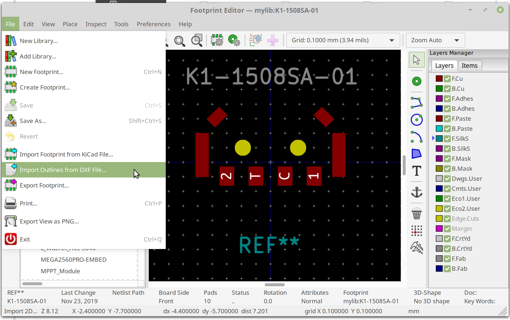
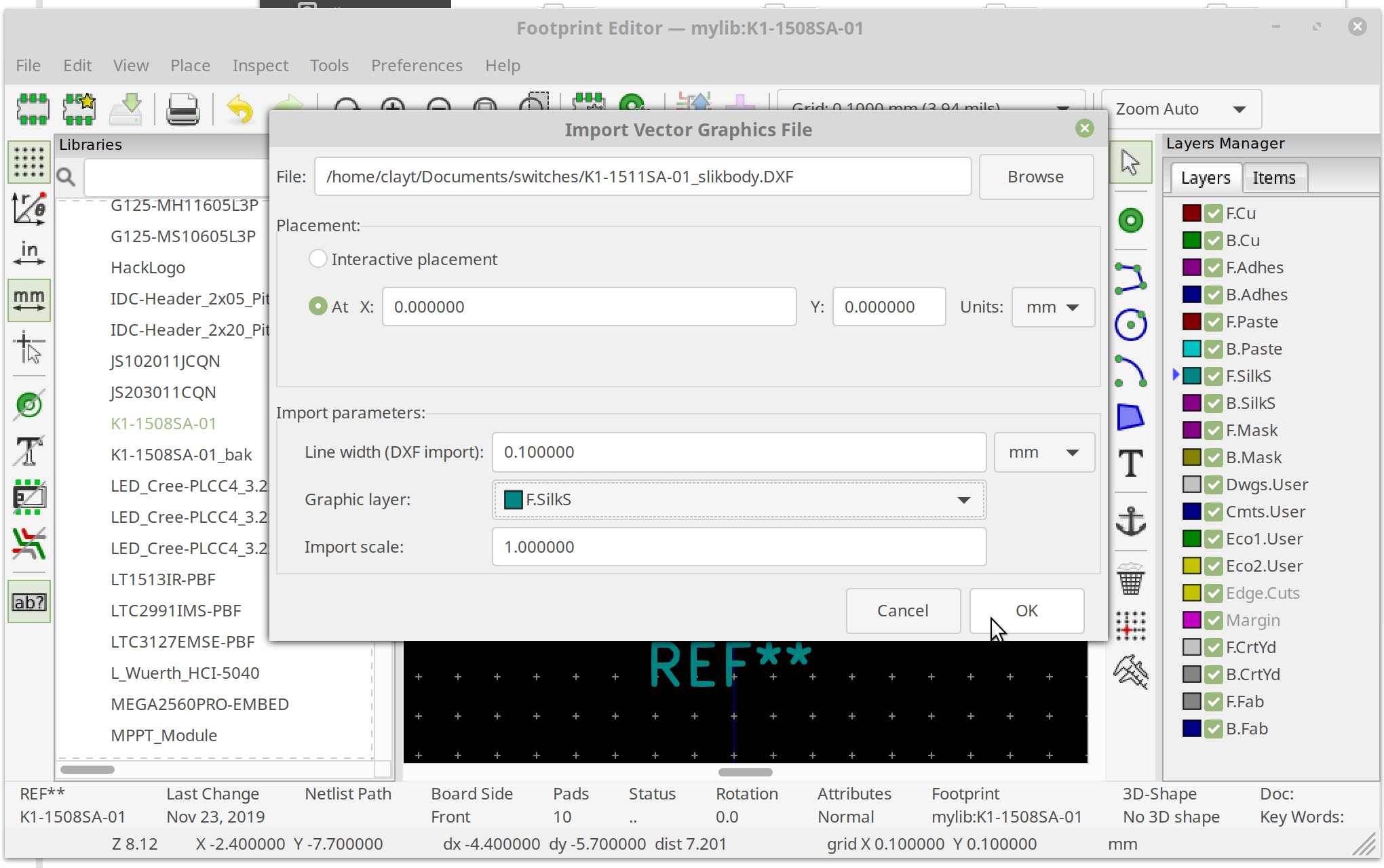
Importing DXF from SolidWorks
KiCad 5 has made this process super easy and straightforward, given one is able to export the DXF nicely. Specifically, I am running KiCad Version: 5.1.5-52549c5~84~ubuntu18.04.1, release build.
KiCad Split Lines at Cursor
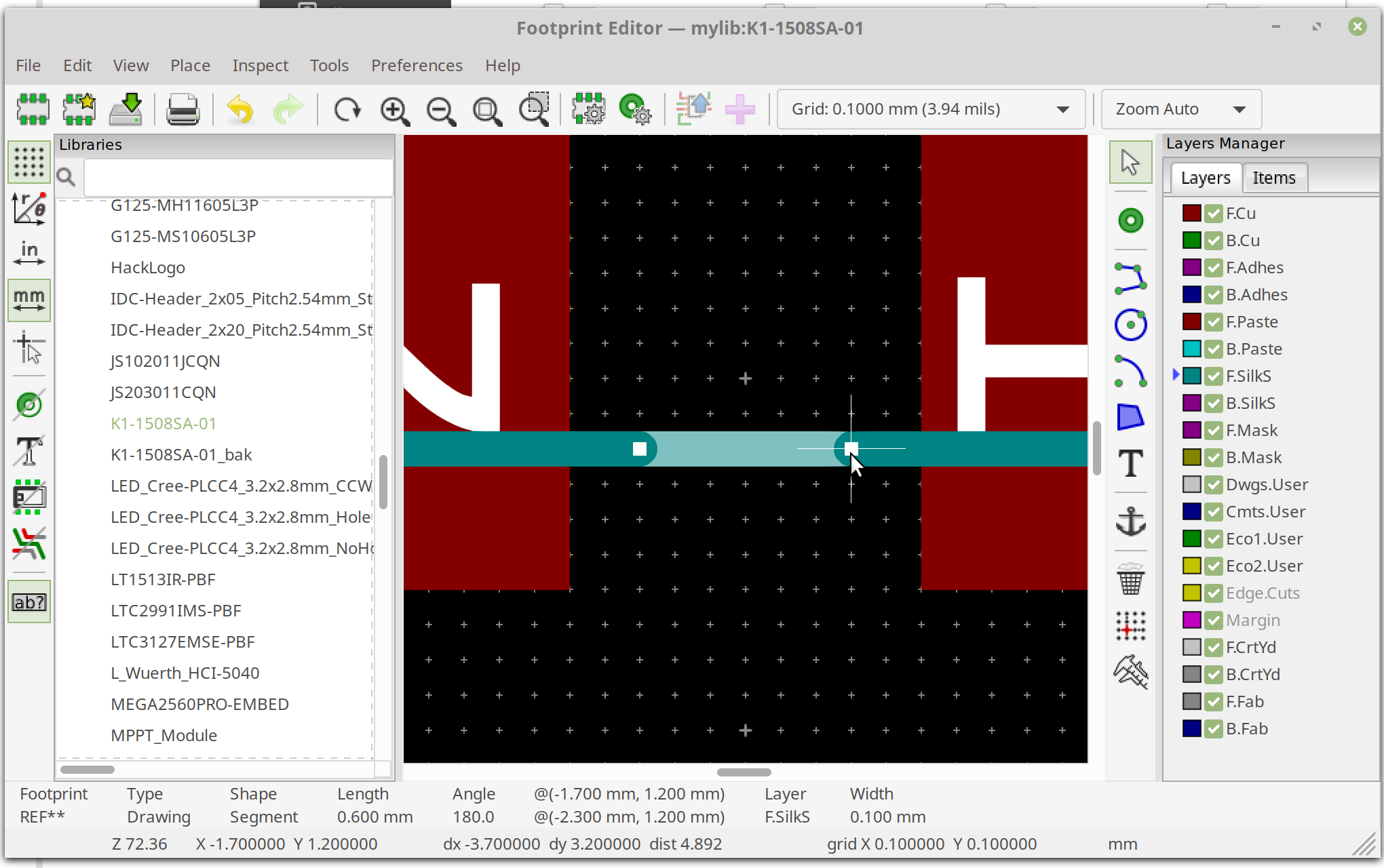
To avoid DRC (Design Rule Checker) errors one must remove the silkscreen over the copper pads. Most board houses will remove the silkscreen (assuming it would even stick) but it is still bad practice to leave it behind. See KiCad Library Convention (KLC): F5.1 - Silkscreen layer requirements Item #3.
There exists a "Create Corner" feature that will add a corner point to the selected line segment nearest the cursor. The shortcut is the Insert key.
Note: Through writing this post and reopening the file I noticed there is a bug in ModEdit. See the launchpad bug report for more information.
Finishing Up
This is pretty wrapped up for now. I will whip up a quick schematic symbol to accompany the footprint. Once that is done, the K1-1508SA-01 is well on it's way to being used in several of my designs.